- InVia confocal Raman microscope
- Rigaku SMARTLAB X- RAY DIFFRACTOMETER
- FEI mod. QUANTA INSPECT 200 LV: SEM with EDS

InVia confocal Raman microscope
High resolution modular system connectable with microscope, instrument that provides information on the molecular composition, bonds, chemical environment, phase and crystalline structure of the samples under examination, and is therefore suitable for the analysis of materials in various forms: gas , amorphous or crystalline liquids and solids. The apparatus is equipped with three laser beams: 532 nm, 632.8 nm, e 785 nm connected with a microscope in reflection and transmission mode in 10X 20X, 50X and 100X -ULWD.

Rigaku SMARTLAB X- RAY DIFFRACTOMETER
Rigaku Smartlab diffractometer, high resolution theta-theta multifunctional X-ray for powders and masses. X-ray diffractometry is the ideal method for obtaining information on the structures of crystalline materials on an atomic scale and in minerals and rocks. In particular, powder diffraction allows for a qualitative and quantitative analysis of the mineralogical composition of the investigated material. The instrument consists of: a high resolution theta-theta geometry vertical goniometer with movement of the coupled and / or independent axes, with angular range between -10 ° and + 160 ° in 2-Theta and minimum step of 0.0002 ° 2 theta; a continuous high frequency 3kW X-ray generator, capable of delivering a voltage between 20 and 50kV, in 1kV steps, and a current between 5 and 60mA, in 1mA steps, with stability of at least ± 0.01 % for input variations of ± 10% in voltage and current, complete with protective hood for X-ray tube with electromagnetic shutter managed by software.

FEI mod. QUANTA INSPECT 200 LV: SEM with EDS
SEM with EDS for scanning electron microscopy and elemental analysis. SEM scanning electron microscopy system of the FEI mod. QUANTA INSPECT 200 LV with EDS analysis system: EDAX GENESIS with SUTW detector for the acquisition of spectra.

QUORUM Q150R S: sputter coater
Sputter coater for samples preparation to be analyzed by SEM with 18 stations per stub.

Optical Microscopy
- 5x, 10x, 20x and 100x optics
- up to 1000x real magnification (with CCD contribution)
- PC interfaced for X-Y measurements
- X-Y motorized stage for automated analysis (10 um resolution)
- Z manual stage (0.1 um resolution)

Microfluidic test bench
Home assembled characterization setup for full microfluidic test procedures (mixing, microchannels sealing, max pressure, fluid control, particle tracking, filtering, ...) and customized microfluidic assembly.
It is equipped with optical microscope (Leica DVM2500), motorised syringes (Harvard 33 Dual Syringe Pump), pressure and temperature sensors, temperature controllers and Thermoelectric Generators (Peltier cells), everything interfaced with a PC with a customised Labview® interface.

FT-IR Spectroscopy
- Wavenumber range 11’700 to 600 cm-1
- ATR in macro (Diamond crystal)
- Multi-bounce (ZnSe)

Optical Contact Angle
This system is suited for the measurement and analysis of:
- the static and dynamic contact angle according to the Sessile and Captive Drop method
- the drop shape according to the Pendant Drop method
- the wetting behaviour on solid surfaces
- the surface free energy of solids and their components
- the surface and interfacial tension out of the analysis of the drop shape


- Potentiostat / galvanostat Metrohm Autolab PGSTAT128 + PC
- Arbin Instrument Testing System model BT-2000 + PC
- Potentiostat / galvanostat Biologic VMP3 + PC
- IPCE: Lamp 100-W QTH (Newport) and monocromator150-mm Czerny Turner (Omni-l 150, Lot-Oriel)
- Sun Simulator Class A, 91195A, Newport
- Keithley 2440 source measure unit + PC
- UV-Lamp (Newport)
- Probe station with micromanipulators
- Glove box in Nitrogen atmosphere for material preparations and electrical measurements (in/out electrical connection)
Precision Source/Measure Unit
Offers the capability to perform DC and pulsed electrical measurements for semiconductor technology development and nanotechnology research. The 2 channels and the high resolution allow measurements of experimental transistors and electrical sensors.
- Mimimum source and measure resolution: 10 fA / 100 nV
- Maximum output: DC: 200 V / 3 A
- Pulse: 200 V / 10 A
The Probe station has a chuck that can support up to 6" wafers with very fine x, y and angular movement. The top microscope allows the correct alignment of the probes with the devices under test. Up to four probes are available, two of them with triaxial cable for extremely precise electrical measurement; the other two have coaxial connections. The Probe station has a soft contact tool that allows a semi-automatic movement to contact the probe tips to the devices without putting too much pressure.
Probe station with puck controlled air-bearing stage:
- 180 x 230 mm (7.1 x 9.1 in) XY total stage movement
- 25 x 25 mm micrometer fine stage movement
- +/- 5 degree fine chuck Theta rotation
- Dedicated 25 mm fine platen height adjustment
- Stable microscope bridge mount
- Vibration absorbing base

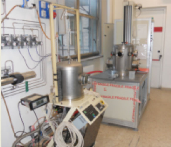
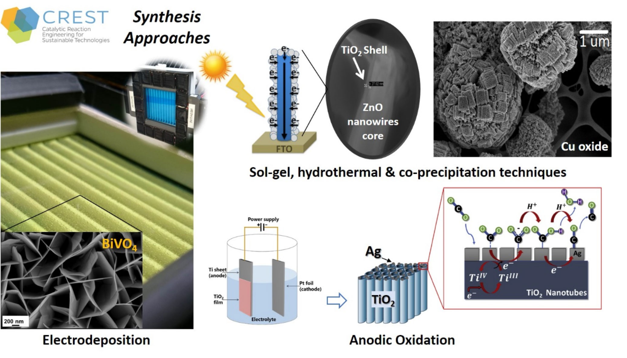
Several equipment’s are available for chemical (co-precipitation, microwave assisted and hydrothermal synthesis, electrodeposition, anodic oxidation, sol-gel and combustion synthesis methods) and physical synthesis (solid-state-reaction, sputtering, etc).
See also:
http://www.disat.polito.it/research/research_groups/crest; http://www.disat.polito.it/research/research_groups/mpmnt.
Several physical-chemical deposition and growth approaches of nanomaterials are available.


Laser-induced graphenization
Laser-induced graphene (LIG) obtained by laser writing of polymeric substrates has been recently reported as an incredibly promising material for flexible electronics. It consists of a three-dimensional network of few layer graphene obtained by a laser writing process of the polymeric surface.
These conductive paths obtained on flexible substrate can be exploited for the fabrication of supercapacitors, batteries, photoelectrochemical solar cells, electrochemical sensors and many other devices that can take advantage from a porous high-surface-area graphene-based network on polymeric substrate.


Electrospun Nanofibers
Through electrospinning technique, non-woven dried nanofiber mats are collected on the counter electrode.
The key advantages of such technology are: i) the polymer can be arranged in a micro/macro porous structure, providing a high surface area to volume ratio; ii) the possibility to collect nanofiber mats, based on several kinds of materials, such as ceramic or carbon based materials, obtained by electrospinning and implementing successively a proper heating treatment; iii) the tuning of ordered distributions of nanofibers, obtained by modulating the electric field during the process
Thin film deposition
Technologies for the growth of thin films both conductive and dielectric (thermal and e-gun evaporation of metals, Plasma Enhanced Chemical Vapor Deposition (PECVD), Low Pressure Chemical Vapor Deposition (LPCVD), magnetron sputtering, silicon oxidation, Electroplating, Rapid Thermal Annealing (RTA)) or active materials (magnetic, piezoelectric by sol-gel deposition or sputtering, …);
See also: http://www.disat.polito.it/research/research_groups/mpmnt